- 您现在的位置:买卖IC网 > Sheet目录331 > IR2086STRPBF (International Rectifier)IC DRIVER FULL BRIDGE 16-SOIC
IR2086S(PbF)
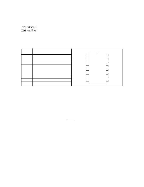
Lead Definitions
Symbol Description
Lead Assignments
VCC
Supply
1
n/c
IR2086S
VB1 16
COM1,2
VB1,2
VS1,2
HO1,2
LO1,2
CT
Supply return
High side floating supply
Floating supply return
High side output
Low side output
Oscillator Input
2
3
4
5
6
7
CS
DELAY
CT
COM1
LO1
VCC
HO1 15
VS1 14
COM2 13
LO2 12
VS 2 11
HO2 10
CS
Current sense input
8
n/c
VB2
9
DELAY
Over current restart delay
Detailed Pin Description
Cs: The input pin to the overcurrent comparator. Exceeding the overcurrent threshold value specified in
“Static Electrical Parameters” Section will terminate output pulses. A new soft start cycle will commence after
the expiration of the programmed delay time at DELAY pin.
DELAY: Delay programming pin for restart after overcurrent condition. A capacitor connected to this pin will
determine the delay form the over current trip to the beginning of a new soft start cycle. The delay time ranges
from 10us to 1s, and is set according to:
t d ≈
C d V cc
2 uA
+ 10 us
CT: The oscillator-programming pin. Only two components are required to program the internal oscillator
frequency: a resistor connected between the Vcc pin and the CT pin, and a capacitor connected from the CT
pin to GND. The approximate oscillator frequency is determined by the following simple formula:
f osc = 1 / (2 · R T · C T )
Where frequency is in Hertz (Hz), R T resistance in Ohms ( ? ) and C T capacitance in Farads (F). The recom-
mended range of timing resistors is between 10k ? and 100k ? and range of time capacitances is between
47pF and 470pF. The timing resistors less than 10k ? should be avoided.
The value of the timing capacitor determines the amount of dead time between the two output drivers: lower
the CT, shorter the dead time and vice versa. It is not recommended to use a timing capacitor below 47pF.
For best performance, keep the time components as close as possible to the IR2086S. Separated ground and
Vdd traces to the timing components are encouraged.
www.irf.com
5
发布紧急采购,3分钟左右您将得到回复。
相关PDF资料
IR2101PBF
IC DRIVER HIGH/LOW SIDE 8DIP
IR2103SPBF
IC DRIVER HALF BRIDGE 600V 8SOIC
IR2104STRPBF
IC DRIVER HIGH/LOW SIDE 8SOIC
IR2105STR
IC DRIVER HALF-BRIDGE 8-SOIC
IR2106PBF
IC DRIVER HIGH/LOW SIDE 8DIP
IR2108PBF
IC DRIVER HALF BRIDGE 8DIP
IR21091STRPBF
IC DRIVER HALF BRIDGE 8SOIC
IR2109STRPBF
IC DRIVER HALF BRIDGE 8SOIC
相关代理商/技术参数
IR-21
制造商:Inter-Market Inc (IMLEC) 功能描述:Unspecified
IR2100A
制造商:未知厂家 制造商全称:未知厂家 功能描述:DC-to-DC Voltage Converter
IR2100A-007
制造商:未知厂家 制造商全称:未知厂家 功能描述:DC-to-DC Voltage Converter
IR2100A-008
制造商:未知厂家 制造商全称:未知厂家 功能描述:DC-to-DC Voltage Converter
IR2100K
制造商:未知厂家 制造商全称:未知厂家 功能描述:DC-to-DC Voltage Converter
IR2101
功能描述:IC DRIVER HIGH/LOW SIDE 8-DIP RoHS:否 类别:集成电路 (IC) >> PMIC - MOSFET,电桥驱动器 - 外部开关 系列:- 标准包装:50 系列:- 配置:高端 输入类型:非反相 延迟时间:200ns 电流 - 峰:250mA 配置数:1 输出数:1 高端电压 - 最大(自引导启动):600V 电源电压:12 V ~ 20 V 工作温度:-40°C ~ 125°C 安装类型:通孔 封装/外壳:8-DIP(0.300",7.62mm) 供应商设备封装:8-DIP 包装:管件 其它名称:*IR2127
IR2101_04
制造商:IRF 制造商全称:International Rectifier 功能描述:HIGH AND LOW SIDE DRIVER
IR21014
制造商:IRF 制造商全称:International Rectifier 功能描述:HIGH AND LOW SIDE DRIVER
